Tiny1-C is a long-wave infrared (8°~14μm, LWIR) thermal imaging module that converts the thermal radiation of objects into images and temperature data. This product is compact, lightweight, energy-efficient, and delivers high-quality images. It is ideal for applications such as industrial temperature measurement, security monitoring, intelligent IoT, and other fields.
Table 2-1. Tiny1-C Product Model Number Explanation (EX: Tiny1C-256-02011X-H-WR-XX)
| Tiny1-C | Resolution | Lens | Gain | Temp Measurement Type | Expansion Card |
|---|---|---|---|---|---|
| Tiny1-C | 256×192 / 160×120 |
02011X: 2.0mm F1.1 03211X: 3.2mm F1.1 04312X: 4.3mm F1.2 |
H: High-quality S: High-quality / Wide-range (configurable) |
WR: Industrial temperature measurement | XX: Standard NF: Near Field |
NOTES
Table 2-2. List of recommended models for Tiny1-C
| NO. | Model Number | Features |
|---|---|---|
| 1 | Tiny1-C256 02011X S WR XX | Large FOV (Field of View) |
| 2 | Tiny1-C256 03211X S WR XX | Standard |
| 3 | Tiny1-C256 04312X S WR XX | Small FOV (Field of View) |
| 4 | Tiny1-C256 03211X S WR NF | Support imaging of close-ups |
NOTE: If necessary, you can contact our company to customize the selection combination that is not recommended in the list.
Table 2-3. Tiny1-C Lens Parameters
| Lens Code | Lens Parameters | Focus | Detection Distance | Recognition Distance | Identification Distance | Temperature Correction |
|---|---|---|---|---|---|---|
| 02011X |
Focal length: 2.0mm F-number: 1.1 FOV: 90°×65° / 54°×40° IFOV: 6mrad |
0.1m~∞ | 200m | 50m | 25m | 0.25m~2m |
| 03211X |
Focal length: 3.2mm F-number: 1.1 FOV: 56°×42° / 35°×27° IFOV: 3.75mrad |
0.25m~∞ | 320m | 80m | 40m | 0.25m~5m |
| 04312X |
Focal length: 4.3mm F-number: 1.2 FOV: 40°×30° / 25°×19° IFOV: 2.79mrad |
0.40m~∞ | 430m | 108m | 54m | 0.25m~5m |
| 03211X-NF |
Focal length: 3.2mm F-number: 1.1 FOV: 56°×42° / 35°×27° IFOV: 3.75mrad |
0.08m~0.13m | - | - | - | - |
NOTES
Table 3-1. Tiny1-C System Specifications
| Detector | Vanadium Oxide Uncooled Infrared Focal Plane Detector |
| IR wavelength | 8~14μm |
| Resolution | 256×192 / 160×120 |
| Pixel pitch | 12μm |
| Noise Equivalent Temperature Difference (NETD) | <50mK @25°C, F#1.0, 25Hz |
| Thermal time constant | <10ms |
| Detector framerate | ≤25Hz |
| Non-uniformity correction | Auto shutter correction |
| Image output formats | 10bit / 14bit |
| Focus method | Fixed focus |
| Temperature measurement range | -15°C~150°C (high quality) 50°C~550°C (wide range) |
| Temperature measurement accuracy | ±2°C or ±2% (typ.) |
| Body temperature detection | Supported |
| Video interfaces | 3.3V, 5V |
| Control interface | SPI / DVP |
| Typical power consumption | I2C |
| Normal mode | 240mW (typ.) |
| Peak (shutter power consumption) | 600mW (typ.) |
| Core dimensions (w×h×l) | 13.2mm×13.2mm×8.5mm (see mechanical drawings) |
| Operating temperature range | Imaging: -40°C~80°C Temperature measurement: -10°C~75°C |
| Storage temperature range | -45°C~85°C |
| Shock | 25g, 11ms, half sine wave, 3 axes |
NOTES
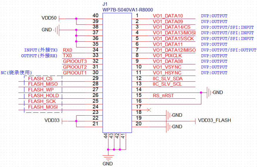
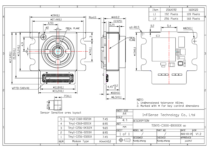
Figure 4-1. Tiny1-C PIN diagram
| No. | Name | Type | Description |
|---|---|---|---|
| 39, 40 | VDD50 | POWER | Analog Power Supply, 5V |
| 35, 36, 37, 38 | GND | GND | GND |
| 34 | UART_RX | IN | UART for debug, 3.3V |
| 33 | UART_TX | OUT | UART for debug, 3.3V |
| 32 | GPIO3 | I/O | Definable GPIO pin, 3.3V |
| 31 | GPIO2 | I/O | Definable GPIO pin, 3.3V |
| 30 | GPIO1 | I/O | Definable GPIO pin, 3.3V |
| 24–29 | RESERVED | NC | NC, for burning the flash |
| 21–23 | VDD3_3 | POWER | Digital Power Supply, 3.3V |
| 20 | GND | GND | GND |
| 19 | VDD3_3_FLASH | POWER | FLASH power supply, 3.3V |
| 15 | RESET_N | IN | Reset signal for module, 3.3V, leave floating if unused |
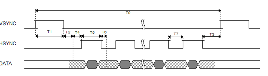
| 11 | V1_HSYNC | OUT | DVP HSYNC |
| 10 | V1_VSYNC | OUT | DVP VSYNC |
| 9 | V1_PIXDAT_8 | OUT | DVP DATA0 |
| 8 | V1_PIXCLK | OUT | DVP clock |
| 7–1 | V1_PIXDAT_12 | OUT | DVP DATA4 |
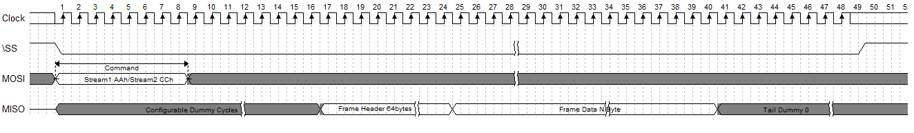
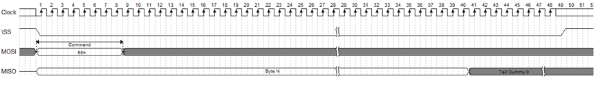
| 7–2 | VOSPI_MISO | OUT | Video Output SPI Signal: MISO |
| 6 | V1_PIXDAT_11 | OUT | DVP DATA3 |
| 5–2 | VOSPI_SCK | IN | Video Output SPI Signal: CLK |
| 3–1 | V1_PIXDAT_14 | OUT | DVP DATA6 |
| 1 | V1_PIXDAT_10 | OUT | DVP DATA2 |
The detector used in the module is sensitive to power supply noise, especially the noise in the analog part, which can directly affect the imaging video. The table below gives the maximum noise, typical working current, and maximum current that the module can tolerate.
| PIN No. | Status | Min. Voltage | Typ. Voltage | Max. Voltage | Typ. Current | Max. Current | Max. Noise (1Hz~50KHz) |
|---|---|---|---|---|---|---|---|
| VDD50 | Normal | 4.5V | 5V | 5.5V | 5.7mA | 23mA | 200μV |
| VDD33 | Normal | 3.15V | 3.3V | 3.45V | 66.7mA | 130mA | 50μV |
| VDD33 | Peak | 3.15V | 3.3V | 3.45V | - | 204mA | - |
We provide the following software and software development resources:
Developers can contact our technical support personnel to obtain the latest version of software development materials.
NOTE: The module itself has no USB interface. When using the module on Windows or using the USB SDK, please connect the development board with a DVP-to-USB converter.
The device control interface adopts standard I2C. The maximum clock frequency is 400KHz, complies with the CCI
protocol in MIPI CSI-2, and the 7bit I2C address is 0111100b (0x3C).
The default output of the module is in "Image" Mode. Customers can switch to "Image + Temperature" Mode through commands or switch to the "Raw Data" Mode if customized algorithm processing or image recognition is needed. Note that "Imaging + Temperature" output at the same frame rate will double the data stream transmitted.
| Mode | Data Type | Data Format |
|---|---|---|
| Image Mode | YUV422 | 256×192 / 160×120 |
| Raw Data Mode | Y14 / Y10 | 256×192 / 160×120 |
| Temperature Mode | Y14 | 256×192 / 160×120 |
| Image + Temperature Mode | YUV422 + Y14 | 256×384 / 160×240 |
Figure 5-1. DVP external synchronization
The VoSPI (Video out SPI interface) uses Motorola’s Serial Peripheral Interface (SPI) and its 4 lines interface protocol. VoSPI defines two commands for reading data:
The command to read a new data frame is used for SPI master to obtain a new image from RS001. When a frame of image is too long to be transmitted at one time, it will continue reading the current frame for the continuation of the previous "reading a new frame of image".
Figure 5-2. Timing diagram: read a new data frame.
Figure 5-3. Timing diagram: continue reading the current data frame.
| Category | Available Functions | Notes |
|---|---|---|
| Imaging | Pseudo color | |
| Zoom | ||
| Flip, rotate, mirror | ||
| 3D digital noise reduction | Temporal Noise Reduction (TNR) and Spatial Noise Reduction (SNR) | |
| Automatic image adjustment | Automatically adjust the image stretching ratio according to the scene, so that the brightness and contrast of the picture are within an appropriate range. | |
| Detail enhancement | Make the edges and details of the image clearer. | |
| Lid pattern noise correction | Eliminate the inherent lid effect of optical system. | |
| Dead pixel correction | Eliminate a single blind pixel in the picture. | |
| Temperature Measurement | Obtain FPA temperature of detector | Determine whether the module is thermally stable and provide reference for subsequent temperature correction. |
| Temperature measurement analysis | Point-line-rectangle temperature measurement; Max/Min temperature measurement. | |
| Temperature measurement alarm * | Remind when the set temperature threshold is exceeded. | |
| Ambient variables correction * | Ambient reflection temperature, atmospheric temperature, target emissivity, and atmospheric transmittance (distance correction). | |
| Secondary calibration for temperature measurement | Recalibrate the temperature deviation caused by optical changes or dissipation structure changes. | |
| Shutter | Manual shutter correction | Through shutter correction, the image is more uniform, and the temperature measurement is more accurate. |
NOTE: Functions with * are only supported by SDK.
| Category | Available Functions | Notes |
|---|---|---|
| Imaging | Pseudo color | |
| Zoom | ||
| Flip, rotate, mirror | ||
| 3D digital noise reduction | Temporal Noise Reduction (TNR) and Spatial Noise Reduction (SNR). | |
| Automatic image adjustment | Automatically adjusts the image stretching ratio according to the scene, ensuring brightness and contrast are within an appropriate range. | |
| Detail enhancement | Enhances edges and details for clearer images. | |
| Lid pattern noise correction | Eliminates the inherent lid effect of the optical system. | |
| Dead pixel correction | Removes single blind pixels from the image. | |
| Temperature Measurement | Obtain FPA temperature of detector | Determines if the module is thermally stable and provides a reference for subsequent temperature correction. |
| Temperature measurement analysis | Point-line-rectangle temperature measurement; Max/Min temperature measurement. Additional functions can be realized via software after acquiring full-frame data. | |
| Temperature measurement alarm* | Alerts when the set temperature threshold is exceeded. | |
| Ambient variables correction* | Corrects ambient reflection temperature, atmospheric temperature, target emissivity, and atmospheric transmittance (distance correction). | |
| Secondary calibration for temperature measurement | Recalibrates temperature deviations caused by optical or dissipation structure changes. | |
| Shutter | Manual shutter correction | Improves image uniformity and temperature measurement accuracy. |
| Automatic shutter setting | Includes automatic shutter switch, time interval setting, and ambient temperature interval setting. | |
| Other Modules | Get product information | Reads data like module SN, PN, and version number for easier product identification and maintenance. |
| Read/Write customized file | Enables reading/writing of customized addresses and lengths for better software recognition. Only available for specified modules. | |
| Firmware upgrade | Sends notifications for firmware upgrades. Supports upgrades after version 3.1. | |
| Configuration switch | Switches between high-quality and wide-range modes. | |
| Burn protection* |
NOTE: Functions marked with * are only supported by the SDK.
NOTE: The drawing below includes example models of the Tiny1-C module. For other models, please contact our technicians for additional information.
During the sample delivery stage of the Tiny1-C module, our company provides a USB kit for demonstration and debugging purposes. Designed by our company, the USB kit includes:
For later USB hardware development, please contact our company to obtain a USB reference scheme or design a USB conversion module independently.
To ensure safety and protect the equipment, please follow these guidelines: